(China (Mainland))

Product Summary
The XC3SD3400A-5CSG484C is a Field-Programmable Gate Array. The XC3SD3400A-5CSG484C is specifically designed to meet the needs of high volume, cost-sensitive consumer electronic applications. The eight-member family offers densities ranging from 50,000 to five million system gates. The XC3SD3400A-5CSG484C builds on the success of the earlier Spartan-IIE family by increasing the amount of logic resources, the capacity of internal RAM, the total number of I/O, and the overall level of performance as well as by improving clock management functions.
Parametrics
XC3SD3400A-5CSG484C absolute maximum ratings: (1)VCCINT Internal supply voltage –0.5 to 1.32V; (2)VCCAUX Auxiliary supply voltage –0.5 to 3.00V; (3)VCCO Output driver supply voltage –0.5 to 3.75V; (4)VREF Input reference voltage –0.5 to VCCO+0.5 V; (5)VIN Voltage applied to all User I/O pins and Dual-Purpose pins. Driver in a high-impedance state: -0.5V to VCCO+0.5 V; (6)Voltage applied to all Dedicated pins:–0.5 VCCAUX+0.5 V; (7)TJ Junction temperature VCCO<3.0V: - 125℃; (8)VCCO>3.0V : -105℃; (9)TSOL Soldering temperature: - 220℃; (10)TSTG Storage temperature: –65℃ to 150℃.
Features
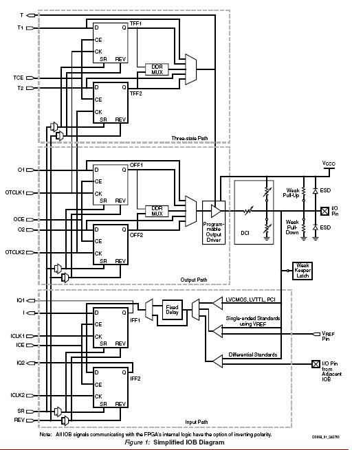
XC3SD3400A-5CSG484C features: (1)Revolutionary 90-nanometer process technology; (2)Very low cost, high-performance logic solution for high-volume, consumer-oriented applications; (3)Densities as high as 74,880 logic cells; (4)326 MHz system clock rate; (5)Three power rails: for core (1.2V), I/Os (1.2V to 3.3V), and auxiliary purposes (2.5V); (6)Select IO signaling; (7)Up to 784 I/O pins; (8)622 Mb/s data transfer rate per I/O; (9)Seventeen single-ended signal standards; (10)Seven differential signal standards including LVDS; (11)Termination by Digitally Controlled Impedance; (12)Signal swing ranging from 1.14V to 3.45V; (13)Double Data Rate (DDR) support; (14)Logic resources; (15)Abundant logic cells with shift register capability; (16)Wide multiplexers; (17)Fast look-ahead carry logic; (18)Dedicated 18 x 18 multipliers; (19)JTAG logic compatible with IEEE 1149.1/1532 specifications; (20)Select RAM hierarchical memory; (21)Up to 1,872Kbits of total block RAM; (22)Up to 520Kbits of total distributed RAM; (23)Digital Clock Manager (up to four DCMs); (24)Clock skew elimination; (25)Frequency synthesis; (26)High resolution phase shifting; (27)Eight global clock lines and abundant routing; (28)Fully supported by Xilinx ISE development system; (29)Synthesis, mapping, placement and routing; (30)Micro Blaze processor, PCI, and other cores.
Diagrams
| Image | Part No | Mfg | Description |  |
Pricing (USD) |
Quantity | ||||||||||
|---|---|---|---|---|---|---|---|---|---|---|---|---|---|---|---|---|
 |
 XC3SD3400A-5CSG484C |
|
SPARTAN-3ADSP FPGA 3400K 484CSA |
Data Sheet |
|
|
||||||||||
| Image | Part No | Mfg | Description | |
Pricing (USD) |
Quantity | ||||||||||
 |
XC3S1000 |
Other |
|
Data Sheet |
Negotiable |
|
||||||||||
|
XC3S1000-4FG456I |
|
IC FPGA SPARTAN 3 456FBGA |
Data Sheet |
|
|
||||||||||
|
XC3S1000-4FG676I |
|
IC FPGA SPARTAN 3 676FBGA |
Data Sheet |
|
|
||||||||||
|
XC3S1000-4FGG320C |
|
SPARTAN-3A FPGA 1M STD 320-FBGA |
Data Sheet |
|
|
||||||||||
|
XC3S1000-4FGG320I |
|
IC SPARTAN-3A FPGA 1M 320-FBGA |
Data Sheet |
|
|
||||||||||
|
XC3S1000-4FGG456C |
|
IC SPARTAN-3 FPGA 1M 456-FBGA |
Data Sheet |
|
|
||||||||||