(China (Mainland))

Product Summary
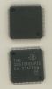
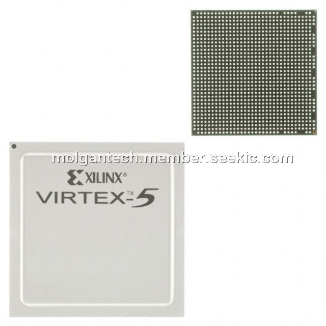
The XC5VLX30T-1FFG665C is a FPGA. It contains platform FPGAs for designs that is based on IP cores and customized modules. The XC5VLX30T-1FFG665C incorporates multi-gigabit transceivers and PowerPC CPU blocks in Virtex-II Pro Series FPGA architecture. It empowers complete solutions for telecommunication, wireless, networking, video, and DSP applications. The leading-edge 0.13 μm CMOS nine-layer copper process and XC5VLX30T-1FFG665C is optimized for high performance designs in a wide range of densities. Combining a wide variety of flexible features and IP cores, the XC5VLX30T-1FFG665C enhances programmable logic design capabilities and is a powerful alternative to mask-programmed gate arrays.
Parametrics
XC5VLX30T-1FFG665C absolute maximum ratings: (1)VCCINT, Internal supply voltage relative to GND: –0.5 to 1.6 V; (2)VCCAUX, Auxiliary supply voltage relative to GND: –0.5 to 3.0 V; (3)VCCO, Output drivers supply voltage relative to GND: –0.5 to 3.75 V; (4)VBATT, Key memory battery backup supply: –0.5 to 4.05 V; (5)VREF, Input reference voltage: –0.3 to 3.75 V; (6)VIN, 3.3V I/O input voltage relative to GND (user and dedicated I/Os): –0.3 to 4.05V; 2.5V or below I/O input voltage relative to GND (user and dedicated I/Os): –0.5 to VCCO + 0.5 V; (7)VTS, Voltage applied to 3-state 3.3V output (user and dedicated I/Os): –0.3 to 4.05V; Voltage applied to 3-state 2.5V or below output (user and dedicated I/Os): –0.5 to VCCO + 0.5 V; (8)AVCCAUXRX, Receive auxilliary supply voltage relative to GNDA (analog ground): –0.5 to 2.0V; (9)AVCCAUXTX, Transmit auxilliary supply voltage relative to GNDA (analog ground): –0.5 to 3.0V; (10)VTRX, Terminal receive supply voltage relative to GND: –0.5 to 3.0V; (11)VTTX, Terminal transmit supply voltage relative to GND: –0.5 to 1.6V; (12)TSTG, Storage temperature (ambient): –65 to +150℃; (13)TJ, Maximum junction temperature: +125℃.
Features
XC5VLX30T-1FFG665C features: (1)25 x 18, two’s complement, multiplication; (2)Optional adder, subtracter, and accumulator; (3)Optional pipelining; (4)Optional bitwise logical functionality; (5)Dedicated cascade connections; (6)SPI and Parallel FLASH interface; (7)Multi-bitstream support with dedicated fallback reconfiguration logic; (8)Auto bus width detection capability; (9)On-chip/Off-chip thermal monitoring; (10)On-chip/Off-chip power supply monitoring; (11)JTAG access to all monitored quantities.
Diagrams
| Image | Part No | Mfg | Description |  |
Pricing (USD) |
Quantity | ||||||
|---|---|---|---|---|---|---|---|---|---|---|---|---|
 |
 XC5VLX30T-1FFG665C |
|
IC FPGA VIRTEX-5 30K 665FCBGA |
Data Sheet |
|
|
||||||
|
XC5VLX30T-1FFG665CES |
|
IC FPGA VIRTEX-5 ES 30K 665FCBGA |
Data Sheet |
Negotiable |
|
||||||